Room 0.28
Staff
Manager: prof. dr hab. inż. Marek Michalik
room: 3.13
phone: +48 604 147 828
e-mail: marek.michalik@uj.edu.pl
dr inż. Irena Brunarska
room: 0.28, 3.23
phone: +48 12 664 43 12; +48 601 501 856
e-mail: irena.brunarska@uj.edu.pl
scientific publications: Irena Brunarska
mgr inż. Anna Łatkiewicz
room: 0.28
phone: 12-664-4312
e-mail: anna.latkiewicz@uj.edu.pl


Equipment
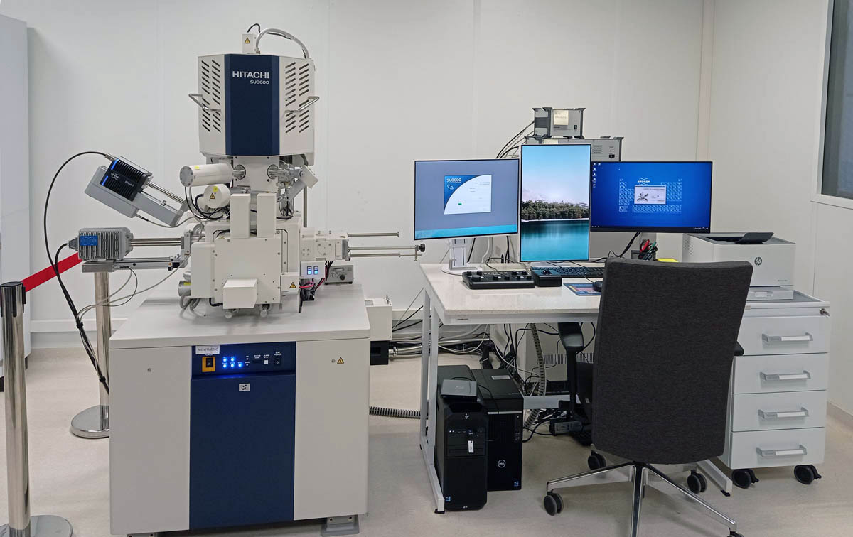
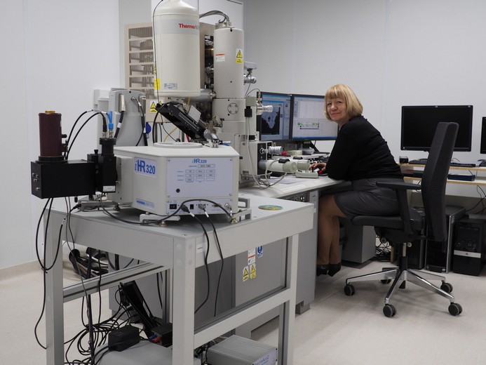
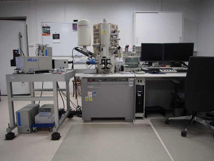
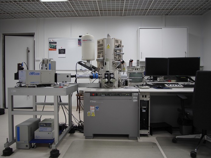
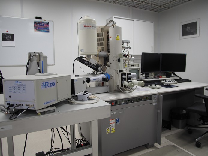
Hitachi SU8600 Cold Field Emission Scanning Electron Microscope with Bruker XFlash 7 and QUANTAX FlatQUAD microanalysis system
The Hitachi SU8600 ultra-high resolution cold field emission scanning electron microscope was installed in November 2023, marking the first Hitachi electron microscope of its class in Poland.

Research Capabilities
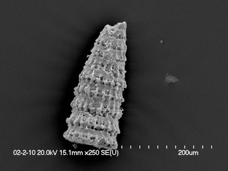
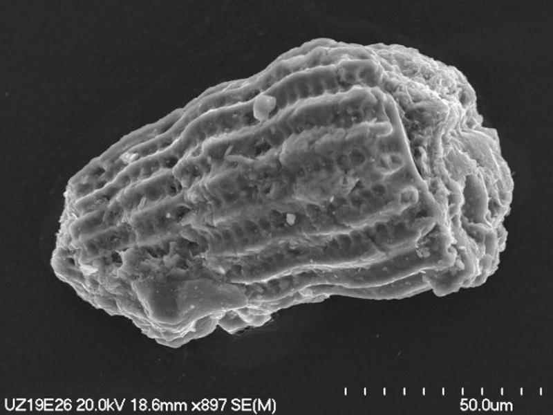
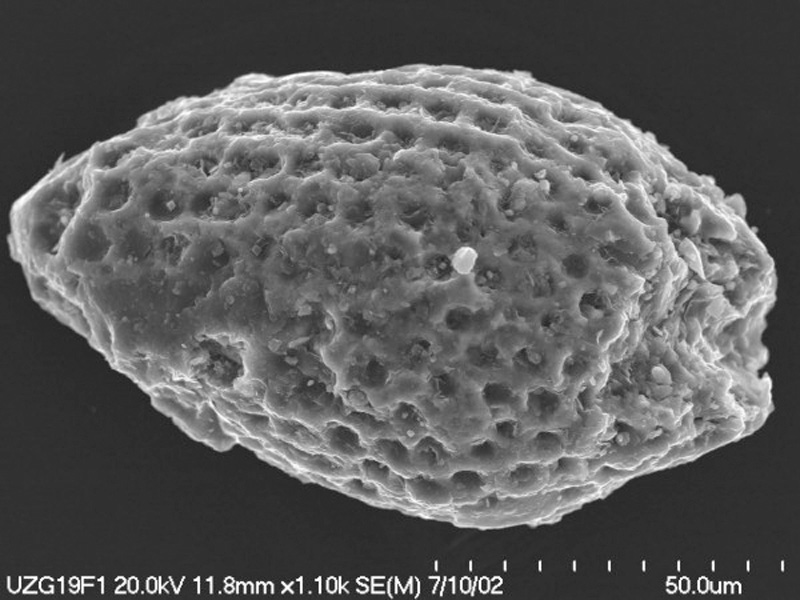
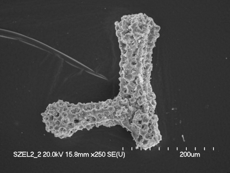
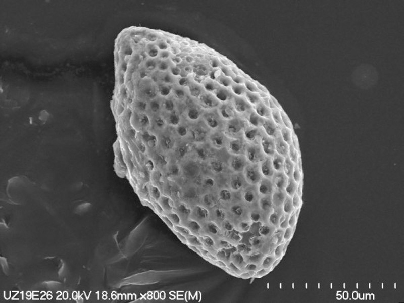
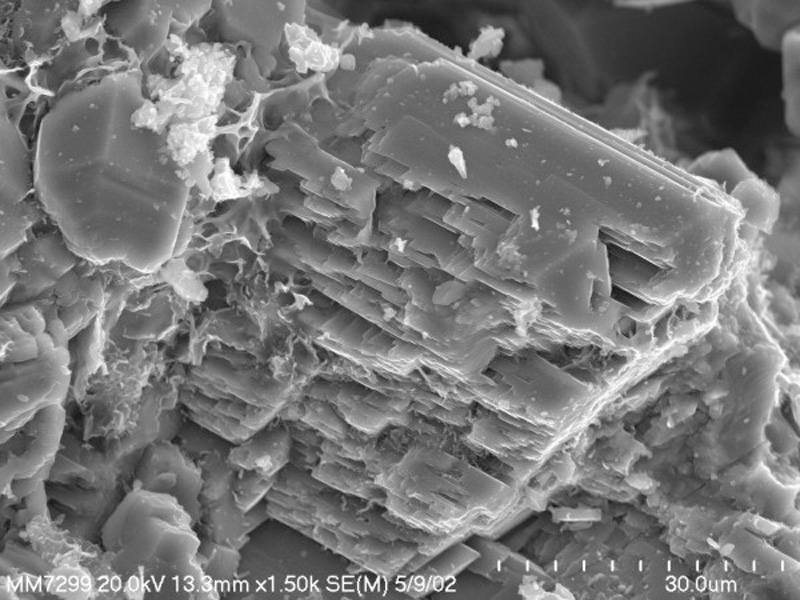
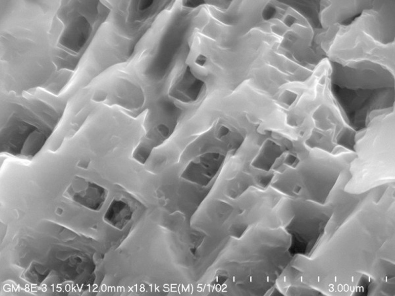
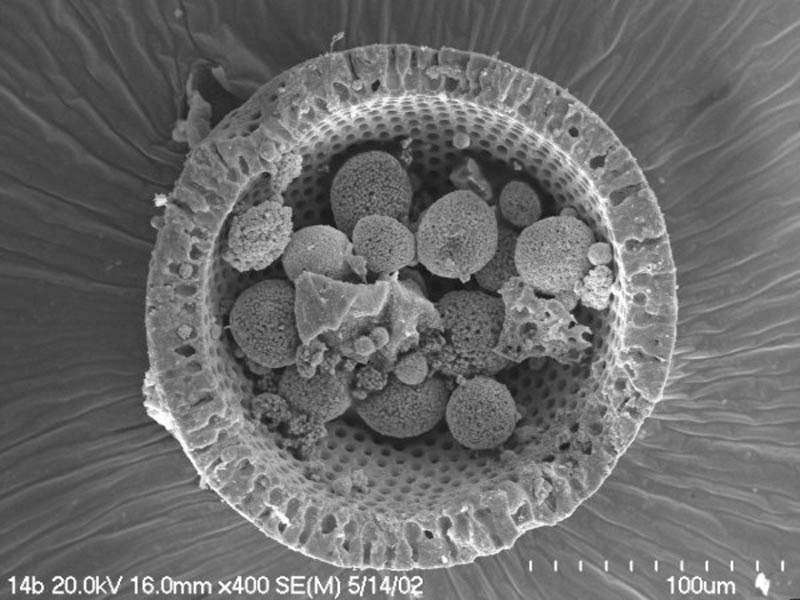
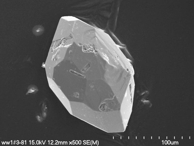
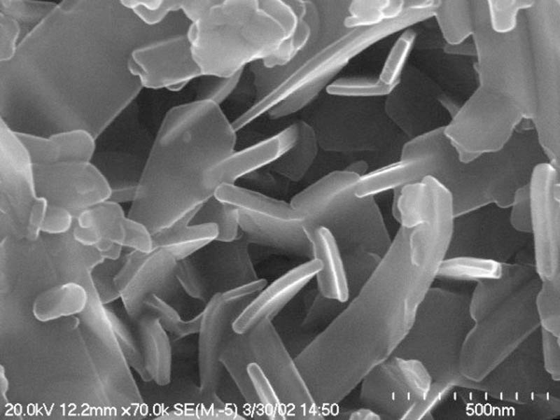
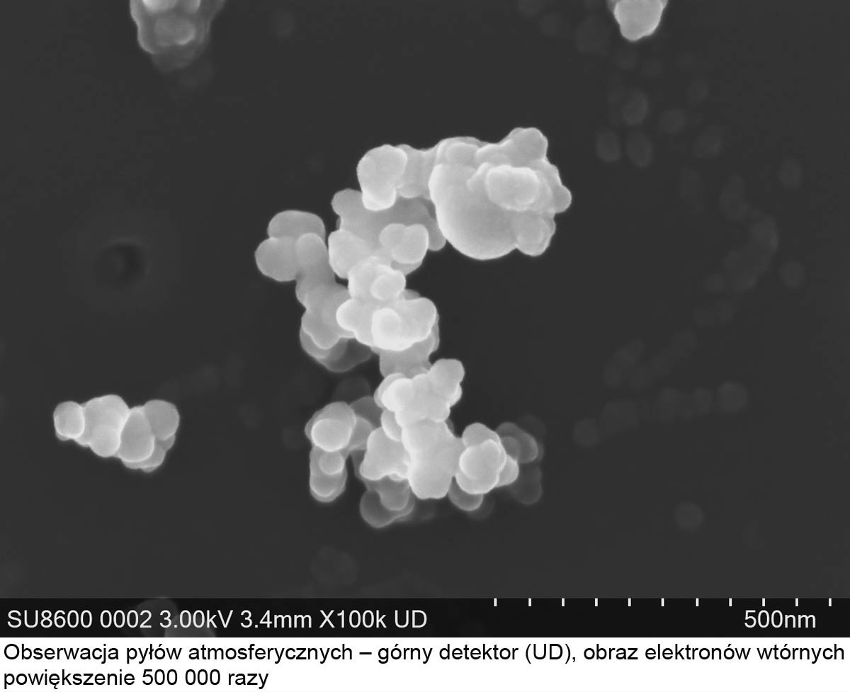
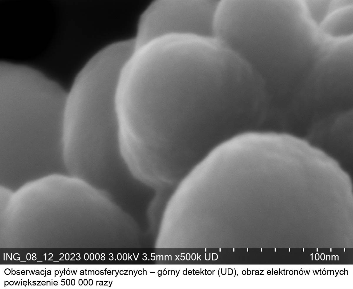
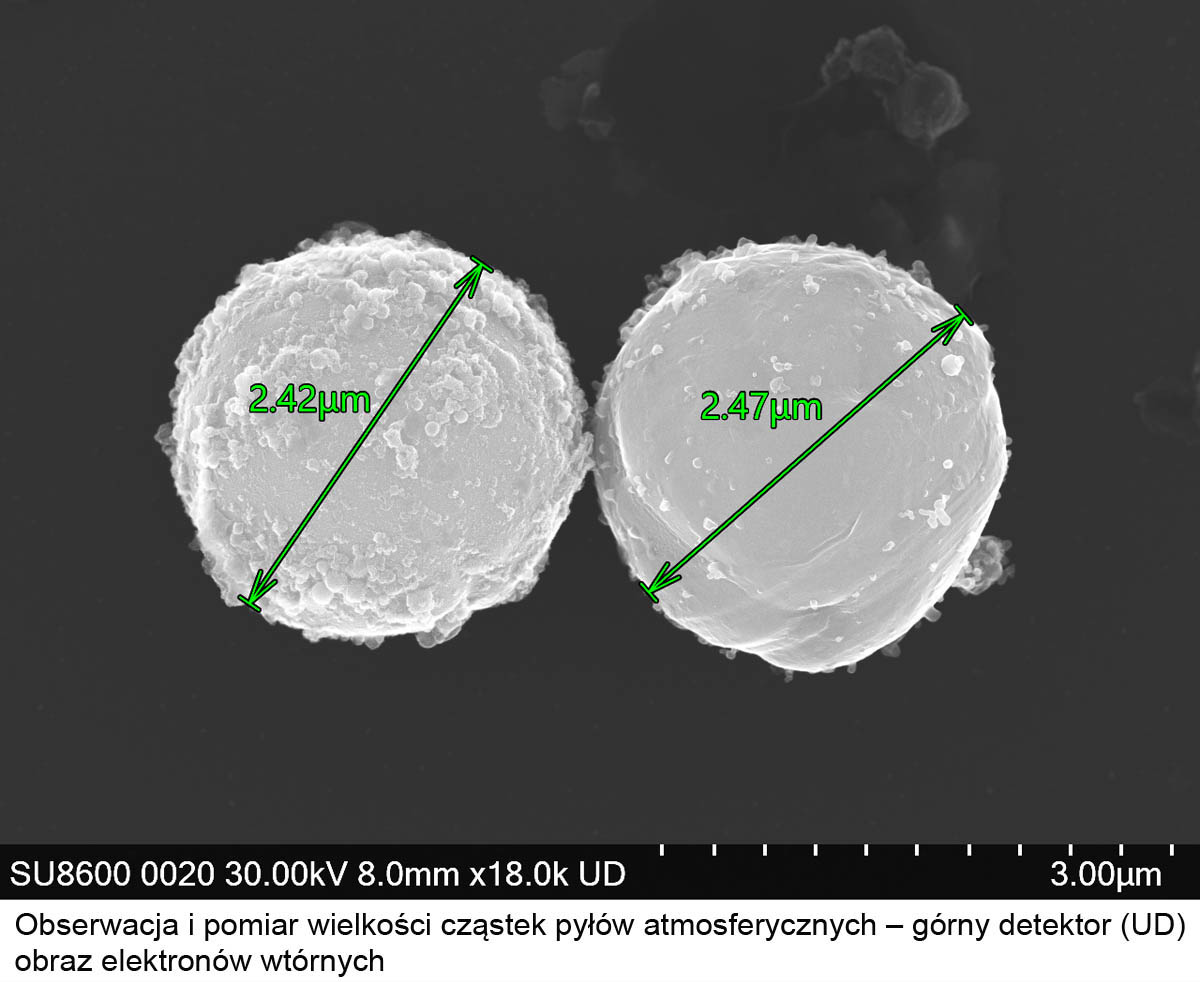
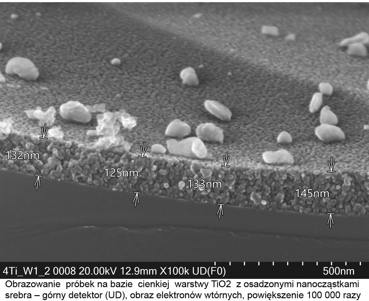
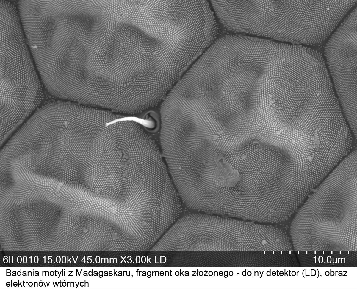
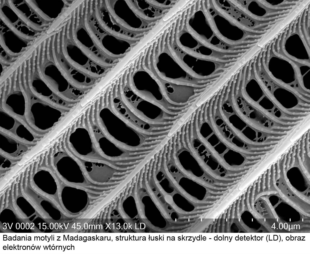
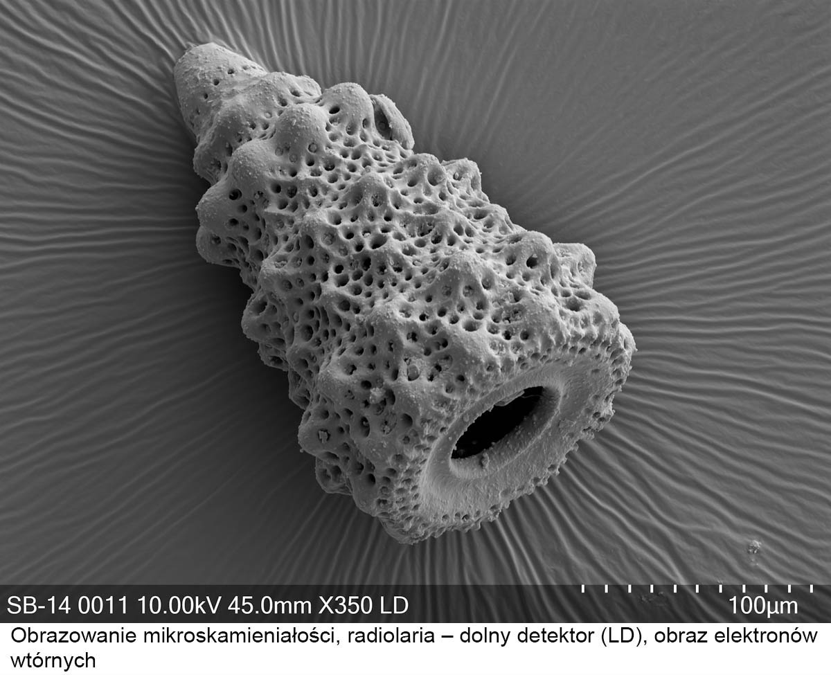
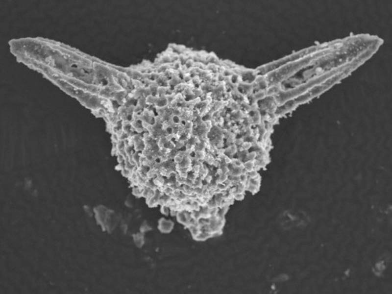
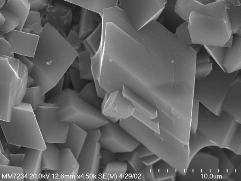
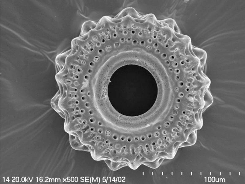
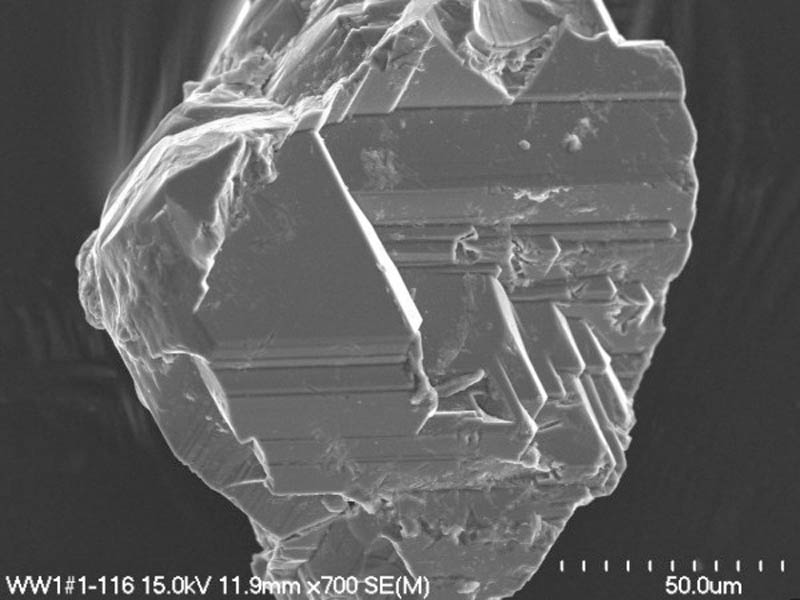
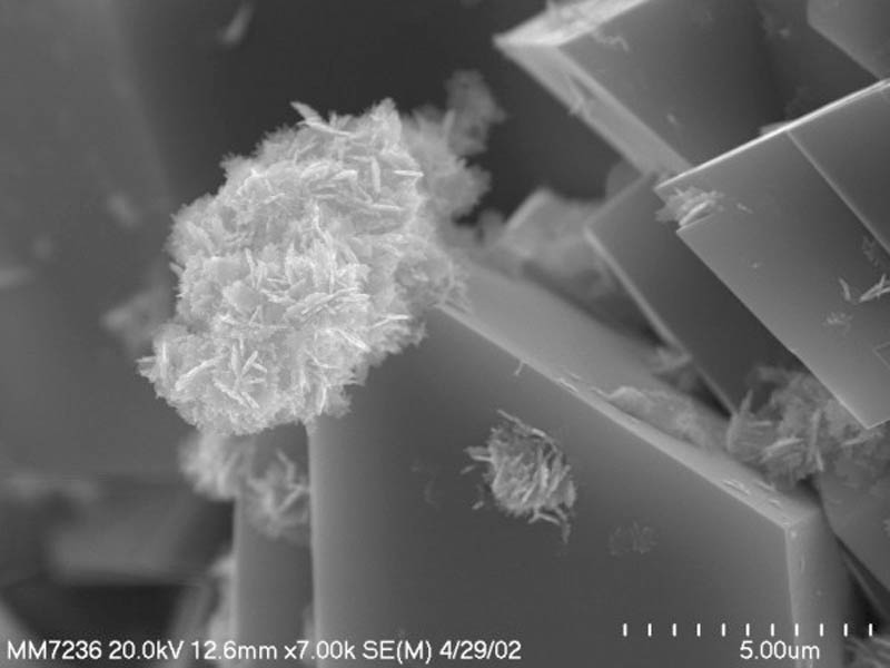
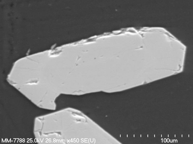
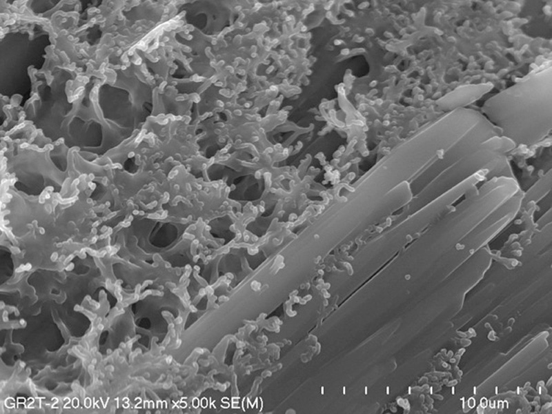
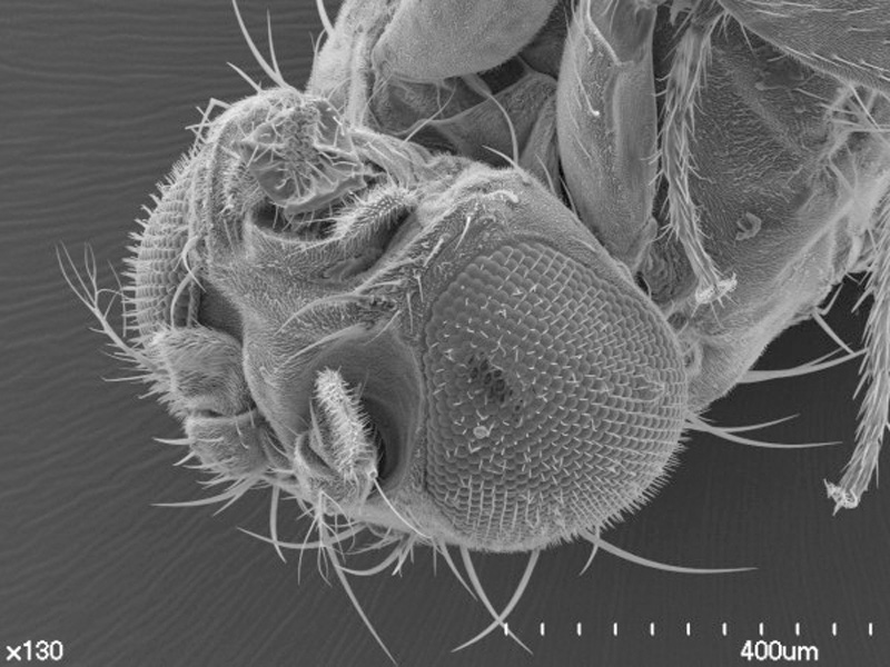
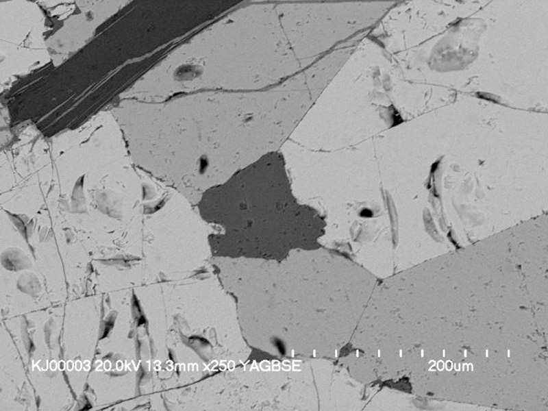
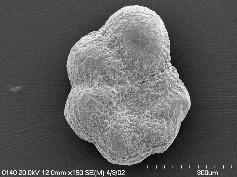
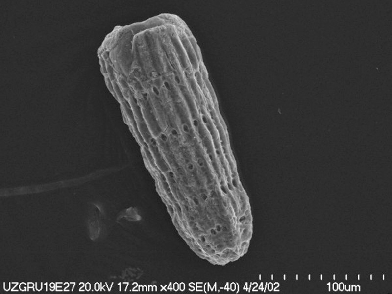
- Imaging of various solid samples at magnifications up to 2,000,000x, including: rocks, minerals, fossils, chemical compounds, dust, powders, alloys, soils, archaeological artifacts, ceramics, properly prepared biological material, composites, aerosols, plastics, and others.
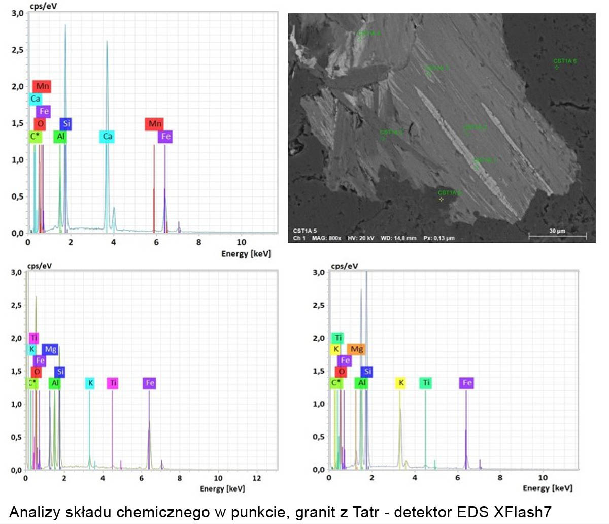
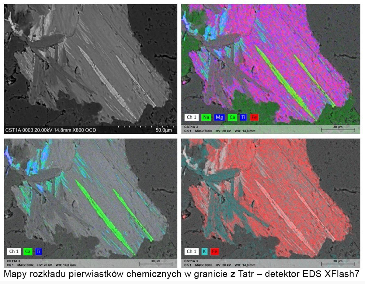
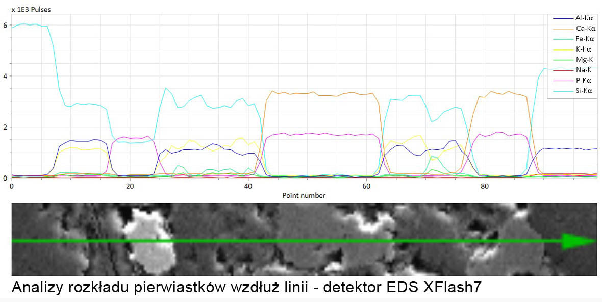
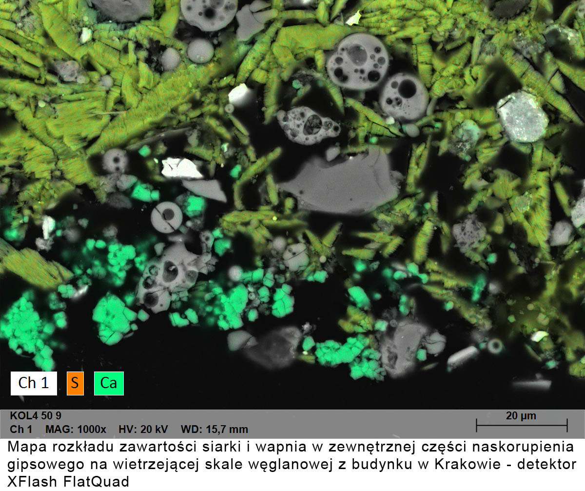
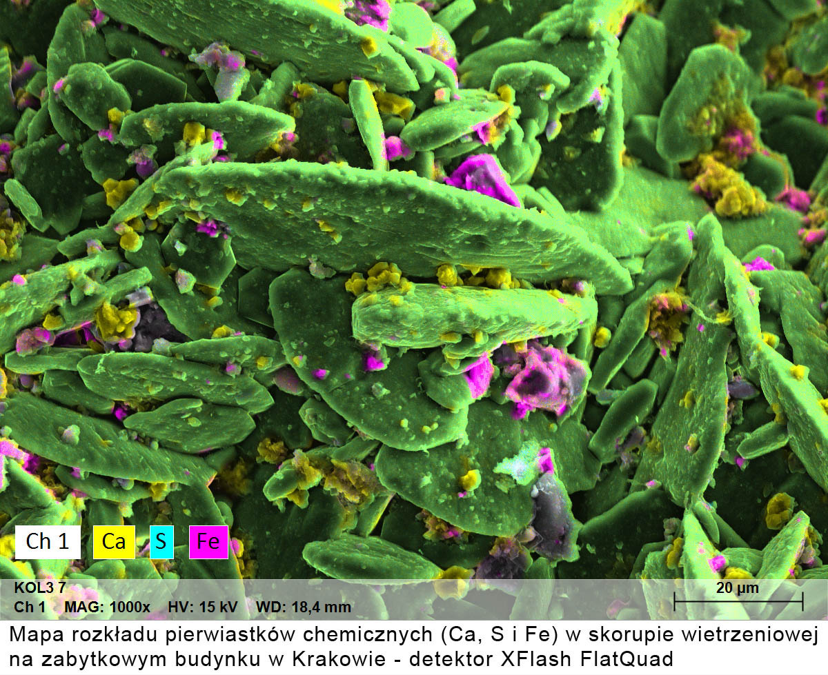
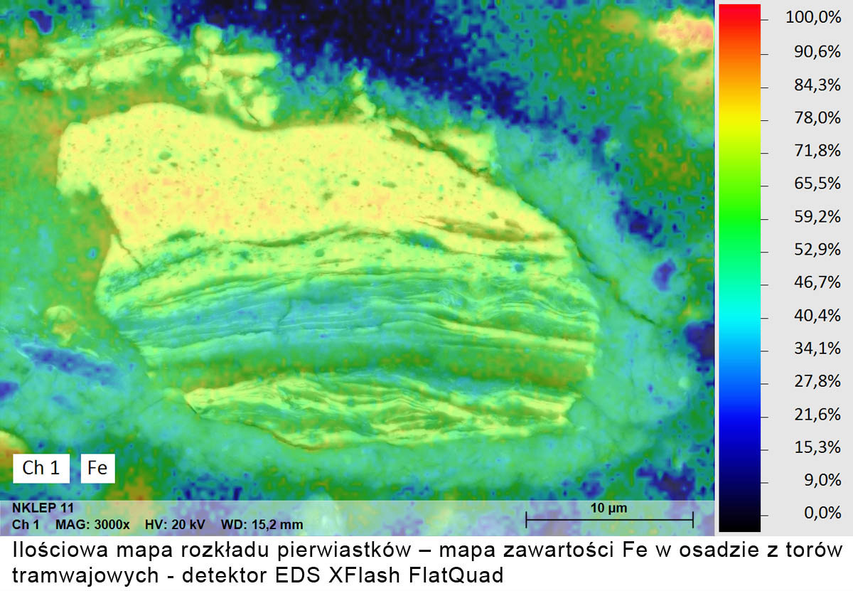
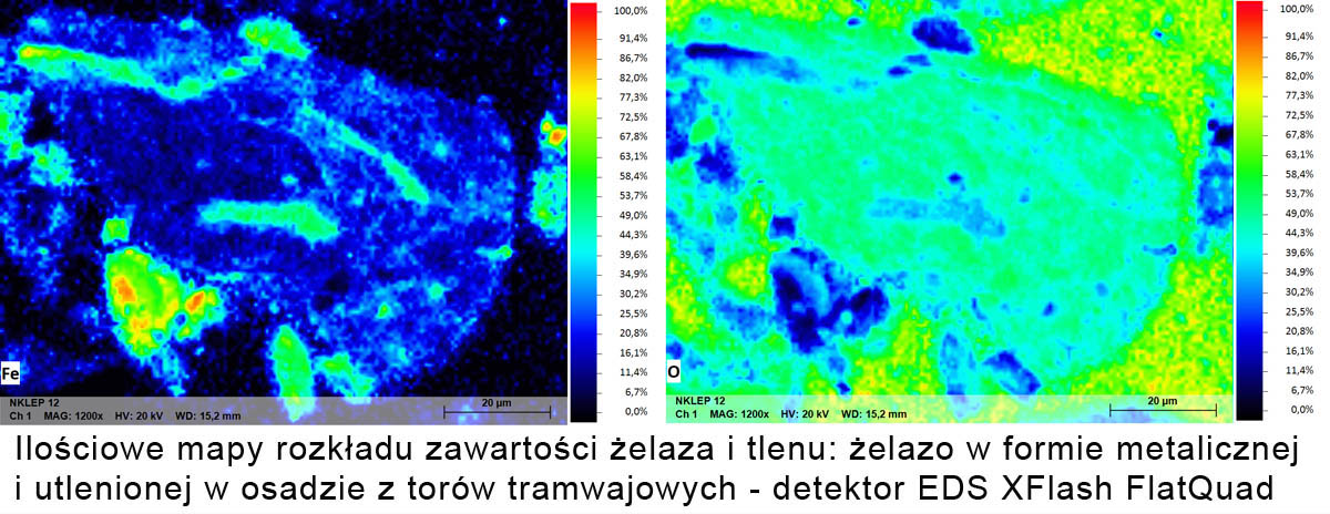
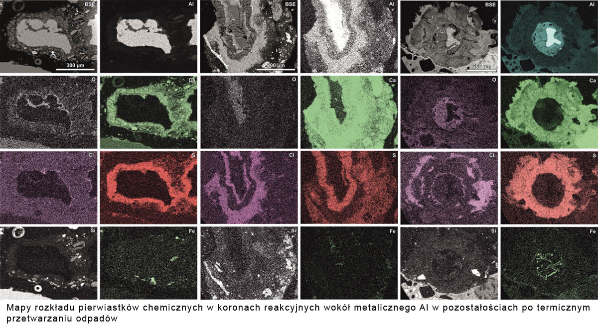
- Ability to perform rapid chemical analysis in microareas - point, line, and area scans, as well as quantitative elemental mapping. We invite all researchers interested in SEM-EDS analysis to collaborate with us.
Characteristics and Technical Parameters:
- Ultra-high resolution (0.6nm at 15kV). A high-brightness cold field emission source from Hitachi provides ultra-high resolution images even at very low voltages (magnification X2000k at 0.80kV).
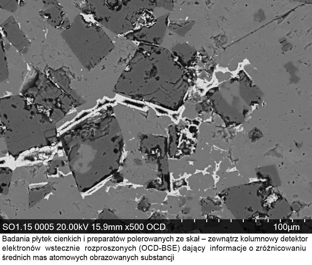
- Five electron signal detectors: secondary electrons (SE) and backscattered electrons (BSE), including an intelligent detection system for low-voltage BSE imaging.
- Fast BSE imaging: a new Out-Column BSED (OCD) scintillator detector.
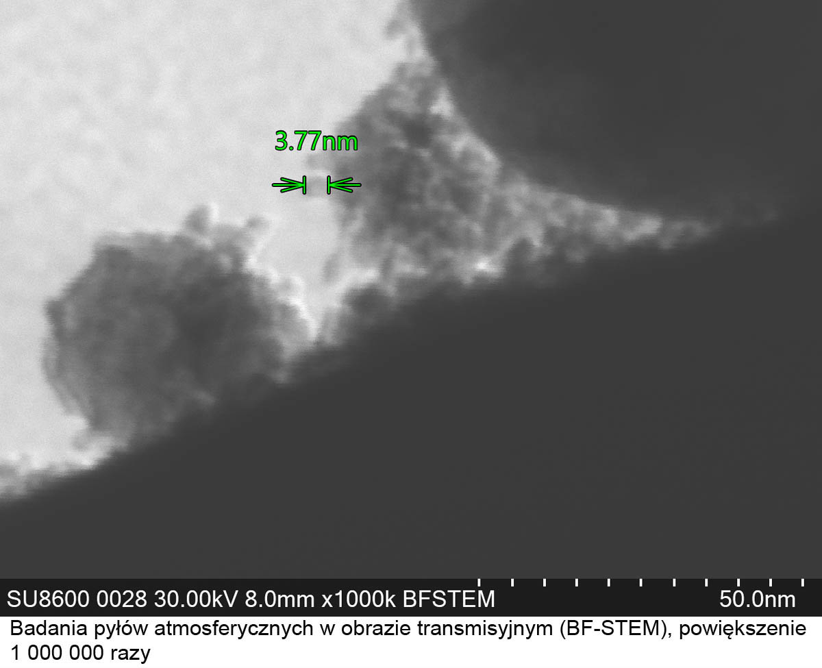
- Transmitted signal detector for bright and dark field STEM imaging (BF and DF STEM).
- Cathodoluminescence detector (CLD).
- EDS XFlash 7 detector enables rapid elemental analysis from Be to Cf.
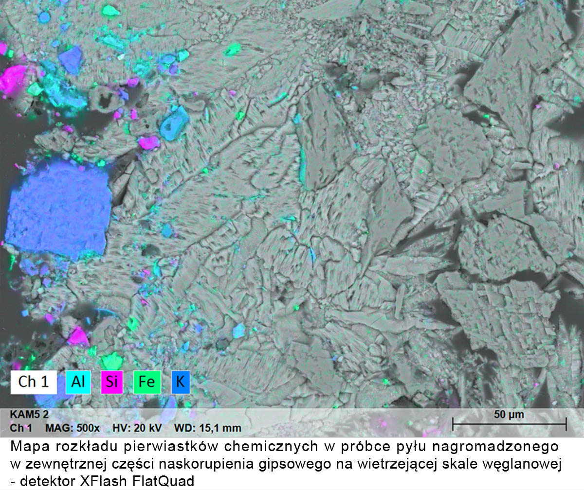
- QUANTAX FlatQuad X-ray detector with high signal acquisition speed, enabling real-time mapping, quantitative mapping, and mapping of samples with varying morphology.
- Spacious sample exchange chamber - the ability to introduce samples with a diameter of up to φ150 mm or several samples at once in the microscope.
- SEM MAP option using a macro image of samples in the chamber for easier navigation.
- Flexible interface - configuration of two monitors allows for simultaneous display and recording of 6 signals to obtain more information in a shorter time. One monitor can simultaneously display 1, 2 or 4 signals, including a view of the entire chamber or SEM MAP.
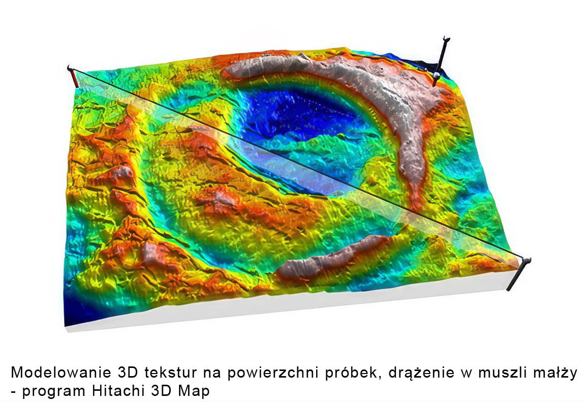
- Hitachi Map 3D image analysis software - 3D texture reconstruction, particle analysis, statistical analysis and classification of particles, measurement of size and orientation of fibers, analysis of EDS maps.
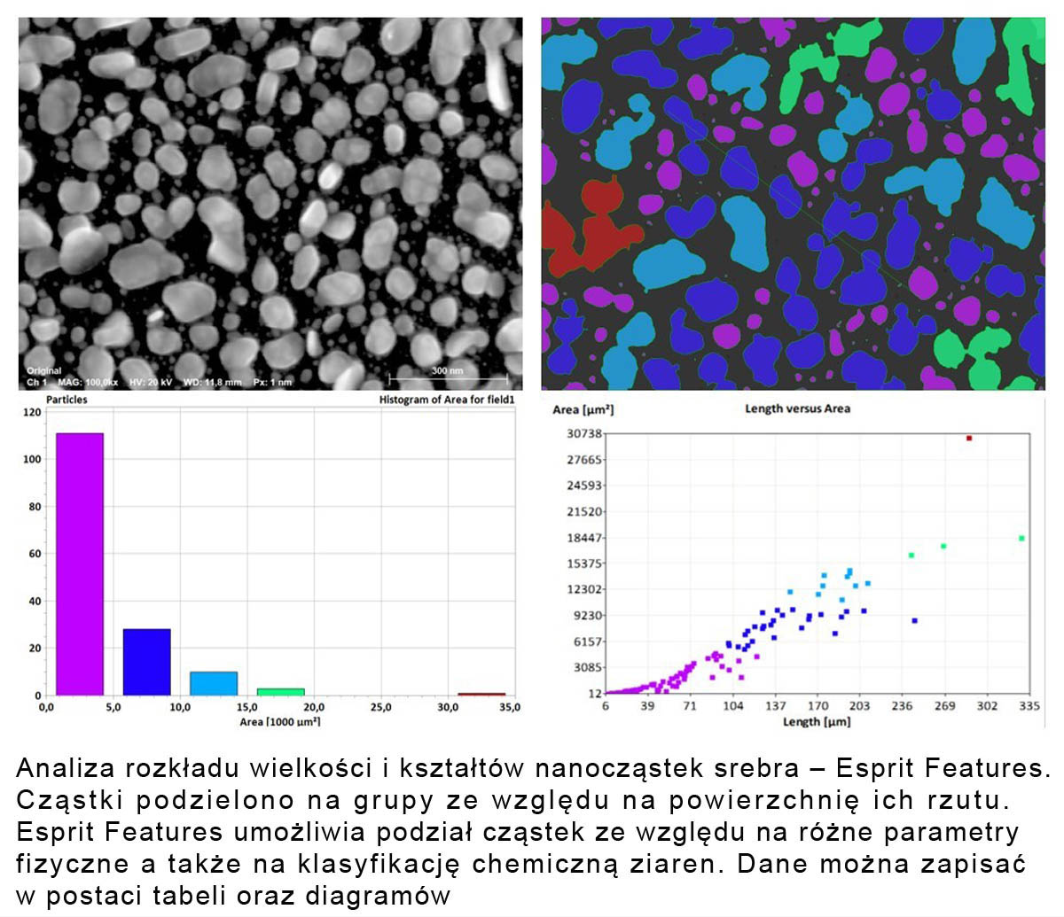
- Esprit Features program enabling statistical analysis of particles with classification based on chemical composition.
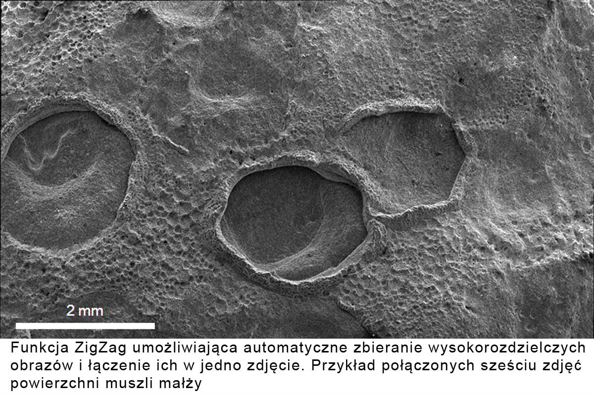
- ZigZag option enabling automatic acquisition of a series of high-resolution images and their combination into a single image.






.jpg)